
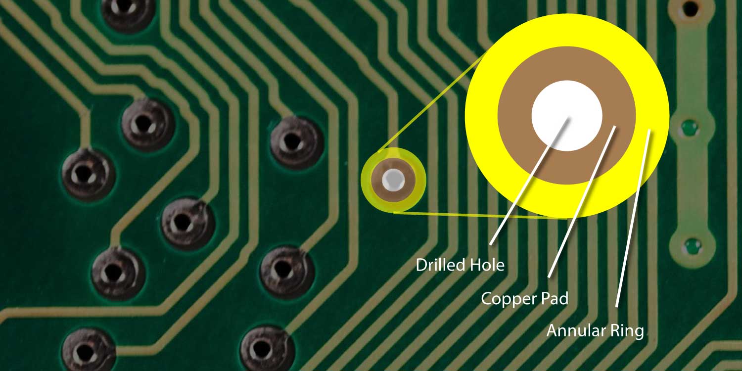
An annular ring derives its name from the shape annulus which means a ring-shaped region. Similar to this, the ring on a printed circuit board (PCB) designates the region between the edge of the conductive copper pad and the drilled hole.
Why do you need an annular ring?
In a PCB, the ring affords room for better electrical connectivity and conductivity in a circuit board. Subsequently, the correct design of an annular PCB ring will have a critical role in the overall functionality of the entire board. The design avoids problems such as tangency and breakouts which negatively affects trace continuity in the entire board.
Determining the annular ring’s width
Calculating the annular PCB ring’s width involves dividing by two the difference between the diameter of the final hole and the diameter of the copper pad.
Ring’s width = [(diameter of the copper pad) – (diameter of the drilled hole)] / 2
To better visualize this, assume the diameter of the copper pad is 20 mil and the diameter of the drilled hole is 8 mil, the width of the annular PCB ring will be 6 mil
Key considerations when designing an annular PCB ring
1- The utility of the Printed Circuit Board
The usefulness of the PCB in the manufacturing of a wide range of electrical appliances implies that the annular PCB ring design will be dependent on the specific purpose for which the PCB is used. Heat transfer, hydraulic, and electrical devices all use circuit boards as seen in home appliances, military, and medical gear. Where smooth electrical communication is prioritized in the PCB, a high-quality ring is designed.
2- The class of PCB product
PCBs are divided into three categories by the Institute of Printed Circuit Boards. These are from classes 1, 2, and 3. The most frequently used PCBs while designing various appliances are Class 3 PCBs. Therefore, compared to class 1 and class 2, class 3 PCBs feature bigger pad sizes and wider annular PCB rings.
3- Cost
An important consideration in the design of annular PCB rings is production cost. The finished product is reasonably priced and lower manufacturing costs are incurred in making small rings. However, the durability of a circuit board seen where in PCB’s rings of significant width needs to be taken into consideration as it will avoid subsequent repair costs.
4- Dense designs
Dense designs refer to a case scenario where the printed circuit board in question is small in size. To economize on space of the copper pad and the via, smaller annular PCB ring sizes are preferred.
5- The drilling accuracy
The ideal location of an annular PCB ring is at the center of the circuit board ensuring equal width across all sides of the ring. The equipment a manufacturer uses to drill a via is a key determinant of the shape and design of the ring and avoids PCB tangency and breakouts.
What is the minimum annular ring width?
The minimum annular ring width accounts for the inner and outer layers of a PCB. The majority of designers concur that the inner layer of a circuit board should have a minimum ring of 0.1mm. The ring’s width on the outer layer synonymous with most PCB designers is 0.05mm.
It is critical to value Design for Manufacturability (DFM) when designing the ring to ensure better connectivity between the multi-layers of the PCBs.
Outer and Inner annular PCB rings
The outer Annular Ring (OAR) is made up of a copper pad. It can be calculated by halving the outer pad diameter.
OAR = (outer copper pad diameter – TOOL SIZE) / 2
In contrast, the area between the solder hole and the outer rim of the copper solder pad is the Inner Annular Ring (IAR). It can be calculated by halving the difference between the inner copper pad diameter
IAR = (inner copper layer pad diameter – TOOL SIZE) / 2
In both cases, the TOOL SIZE is given by:
TOOL SIZE = END SIZE + 0.1mm for whole PTH holes + 0.00mm for complete NPTH holes
The Teardrop Ring versus a through-hole
A through-hole is a PCB packaging technique applicable for electronic components that uses leads on elements inserted into holes in the circuit board. The greatest advantage conferred fewer mistakes and less trouble from unintentionally creating a bridge.
The teardrop ring is the result of drilling misalignment that removed a significant amount of copper from PCB connectors. The advantages of the teardrops include:
- reducing mechanical and thermal stress where a trace connects to a pad.
- lessen the chance that the circuit board will crack.
- Enhance a PCB’s ability to withstand drilling for more comfortable production.
Summary
In conclusion, annular rings are crucial in electrical conductivity and connectivity in the printed circuit pad. A suitable width prevents annular PCB ring tangency and breakout. Tangency occurs when a drill misses the mark resulting in the hole edging toward the pad’s edge. When drilling extends beyond the padded area, this is referred to as a breakout. A breakout can be rectified by adding copper pads in the exposed area in a process called tear-dropping.
About The Author
 Tony Zuberbuehler is a Sales Manager at Versa Electronics with a focus on electronic contract manufacturing. Tony’s career in technology manufacturing spans 25+ years and has included roles as an engineering liaison, in purchasing and material management, manufacturing and planning, customer interfaces, and product fulfillment. Connect with Tony Z on LinkedIn.