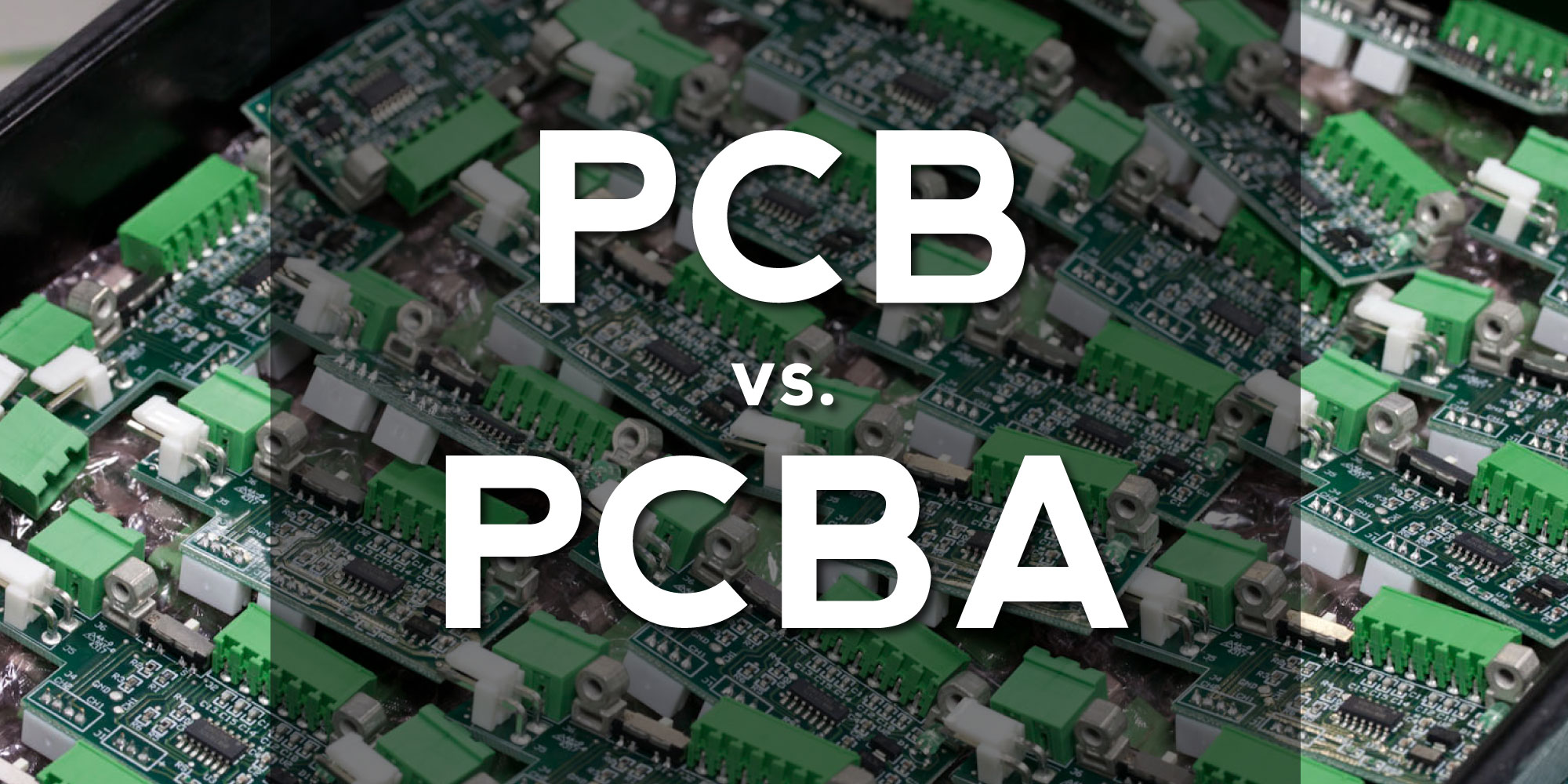
If you are working with electronics, you may have heard the terms printed circuit board (PCB) and printed circuit board assembly (PCBA). While some people use these terms interchangeably, they do not necessarily mean the same thing. So what are they? And what is the difference between PCB and PCBA?
PCB – Printed Circuit Board
A PCB is the mechanical foundation in which electronic components can be mounted to complete an intended circuit. The PCB itself contains a conductive pattern, or trace, and a substrate typically made of glass epoxy resin material. As example, the basic PCB can be divided into 4, 6, or 8 signal layers, with 4 and 6-layer PCBs being the most common. As the name suggests, the PCB pattern is made of a printed component, a printed circuit, or a combination of both. The conductive pattern is either printed or inscribed on an insulating epoxy glass according to the predetermined design.
How is a PCB used?
A PCB can be customized for use in electronic devices like TVs and radios, cell phones, cameras, and computer parts like Motherboard and Graphic cards. PCBs are also used in the manufacture of lighting equipment, medical equipment, automotive industry, and most industrial machinery.
PCB is an essential structure in appliances as it supports the electronic components and serves as an electrical connection for the elements. PCB’s unique features can be summarized as follows:
- High-density wiring, lightweight and small size, which is ideal for miniaturization of the electronic equipment in question
- Due to graphic consistency and repeatability, PBC makes it possible to save on equipment’s maintenance, debugging, and inspection time.
- Its production can be automated to reduce the cost of the electronic appliances
Types of PCB
PCBs come in different forms as follows:
1. Single-layer PCB
Also referred to as single-sided PCB, this is the simplest and the most commonly used PCB in most electronics since it is easy to design and produce. The single-layer PCB is coated with one layer of conducting material, often copper. A layer of solder mask is used to protect the PCB from oxidation. A silkscreen marks the components of the PCB. This type of PCB is used in low cost yet bulk production applications like printers, radio, and calculators.
2. Double-layer PCB
Also known as double-sided PCB, this PCB has a layer of conducting material, usually copper, applied to both the top and bottom sides of the board. The primary advantage of this PCB over its single-sided counterpart is enhanced flexibility and reduced size which makes its circuit compact. It is commonly used in industrial controls, UPS systems, converters, phones, power monitoring units, amplifiers, and HVAC applications.
3. Multi-layer PCB
This type of PCB comes with more than two conductive layers of copper. The board is secured by sandwiching glue between the insulations to ensure that the circuit is not damaged by excess heat. It is used in complex applications like satellite systems, GPS technology, file servers, and data storage equipment and medical equipment.
Other types of PCBs include flexible PCB, rigid PCB, and flex-rigid PCB.
PCBA – Printed Circuit Board Assembly
The abbreviation of printed circuit board +assembly, PCBA is the entire process of passing the unpopulated PCB board through Plated Through Hole (PTH) and Surface Mounted Technology (SMT) processes. These processes provide for all the electronic components to be placed and soldered onto the blank PCB board and include solder paste printing, component placement, hand, wave or reflow soldering and various forms of QC inspection.
Components of PCBA
During an assembling process, an empty PCB board is stuffed or populated with electronic components to form a functioning printed circuit assembly (PCA), or the PCBA. Using through-hole technology, the electronic components become mounted in holes that are surrounded by conductive pads. Using SMT, the components are placed on the PCB to ensure that the pins align with the conductive pads. Where electronic components anchor to either side of the board, the components on one side of the board must adhere to the board by the use of glue before soldering.
A populated PCBA board can be tested using one of the following ways:
- With the power off, the board may be inspected visually or using automated optical inspection tool.
- With the power off, an analog signature analysis can be carried out. This analysis is referred to as “power-off testing.”
- With the power on, in-circuit testing occurs
- Finally, a functional test can be done to establish whether the PCB is doing what it has been designed to do.
From the descriptions above, we can determine that the PCBA refers to a processing flow, or the complete circuit board while the PCB refers to an empty printed circuit board with no electronic components on it. Generally, PCB is a bare board while PCBA is the finished board.
Over 20 Years Of Printed Circuit Board Assembly
Versa Electronics is the experienced supply chain partner for all your electronic manufacturing needs. From surface-mount, through-hole,or mixed technology circuit board and wire harness assemblies to device subassembly and complete product build, Versa delivers quality electronic products for original equipment manufacturers on-time and on-budget.