A strong printed circuit assembly documentation package is one of the simplest ways to improve manufacturing outcomes before production even begins. When the right files are complete, current, and aligned, manufacturers can quote more accurately, launch NPI faster, and reduce the risk of miscommunication during sourcing, assembly, inspection, and test.
Incomplete documentation creates friction. Missing BOM details, unclear assembly drawings, outdated revisions, or inconsistent file sets can all lead to quoting delays, engineering questions, and production issues that cost time and money. By contrast, a clear documentation handoff helps streamline communication and gives your contract manufacturer the information needed to support a smoother build from the start.
Below, we outline the core documentation typically needed to support a successful printed circuit assembly project.
Regardless of the advanced capability of electronic manufacturing service providers, nearly every electronic device will require functional components to manage power, input/output interfaces, and processing. A printed circuit assembly (PCA) is the result of a process to connect these functional electronic components with the wirings of printed circuit boards (PCB). Before these electronic components can be manufactured, standard documentation for a printed circuit assembly must be created.
This article is a guide to printed circuit board assembly documentation that results in a reliable, repeatable, and cost-effective PCA design.
PCA Design Assumptions
For the purposes of this article, we have assumed that the electronic product design and electronic device schematics are validated for purpose and functionality.
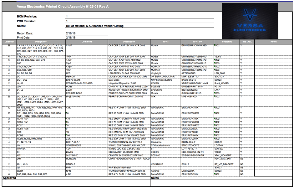
PCA Bill of Materials
While the electronic device schematics are being developed, a product designer will simultaneously develop the bill of material (BOM). The BOM is a listing of the specific electronic components needed to complete the entire printed circuit assembly. Important data recorded on the BOM includes:
- Voltage values
- Values for current
- Tolerance values
- Base part numbers
- Individual part reference designator(s)
- Quantity
- Footprint
- Packaging
PCA Approved Vendor List
While the electronic device schematics and bill of materials are being developed, an electronic product designer will also develop the approved vendor list (AVL). The AVL adds more detail to the bill of materials by specifying an exact manufacturer and manufacturer’s part number for each electronic component line item on the bill of material.
Whether a component is single-source or has multiple sources of supply is a critical consideration. An electronic product designer should make every effort to qualify alternate vendors on the AVL as early as possible. There can be notable repercussions to product cost and delivery if a single electronic component has limited sources or is not available to the electronic manufacturer when needed.
Printed Circuit Assembly Manufacturing Cost & Lead Time
From a manufacturing perspective, the BOM and AVL will involve a high-level of cost and lead-time with respect to purchase and availability at PCA prototype, PCA production, and late-product lifecycle stages. It’s important that the electronic product designer considers electronic material cost, lead-time, and expected longevity for each electronic component defined in the PCA schematic capture and during the development of the PCA bill of material.
Printed Circuit Board
A printed circuit board (PCB) is a primary part on the BOM. The PCB is the “canvas” or substrate that provides electrical connection and mechanical support of all the other components on the printed circuit assembly. The printed circuit board is a custom-fabricated part critical to the performance of the circuit.
The design of printed circuit board and printed circuit assembly is part art and part science. Component placement with a PCA requires much detail and considerations must include:
- Effective electrical connections
- Signal management
- Thermal effects on the component and complete assembly
- Part and connection pad placement for assembly efficiency
- Part and connection pad placement for test and repair
- Electromechanical consequence for input/output connections
- Mounting the PCA into an upper level device
PCB Design and PCB Testing
Training, experience, and automated software suites are important tools for the PCB designer. The process of taking the schematic, BOM, and AVL through the PCB layout process to a finished physical state requires testing and validation. Software that guides a designer and utilizing “Design Rule Checking” software functions help contribute to a quality base circuit, reduced manufacturing cycle times, and improved electronic product quality and reliability. An experienced PCB designer along with PCB software can ultimately provide a more cost effective and repeatable production assembly.
Printed Circuit Assembly Document Package
Once complete the designer will provide a printed circuit board assembly document package to the assembly team at the electronic manufacturing service provider. A comprehensive printed circuit assembly document package typically includes the following:
- Bill of Materials (BOM) – The BOM is the master list of all components needed to build the assembly, including part numbers, descriptions, quantities, and reference designators.
- Approved Vendor List (AVL) – The AVL identifies the approved manufacturers or suppliers for each component to help ensure sourcing consistency, quality, and availability.
- Gerber or Intelligent Manufacturing Data (all required layers, drill, route, and fabrication data) – These files provide the board layout and manufacturing details needed to fabricate the bare PCB accurately.
- CAD data (ODB++ for example) – CAD data gives the manufacturer a more complete digital view of the board design, which can help reduce interpretation errors and improve manufacturing efficiency.
- Pick-and-place / Centroid file – This file shows the location, rotation, and placement side of each component so automated assembly equipment can place parts correctly.
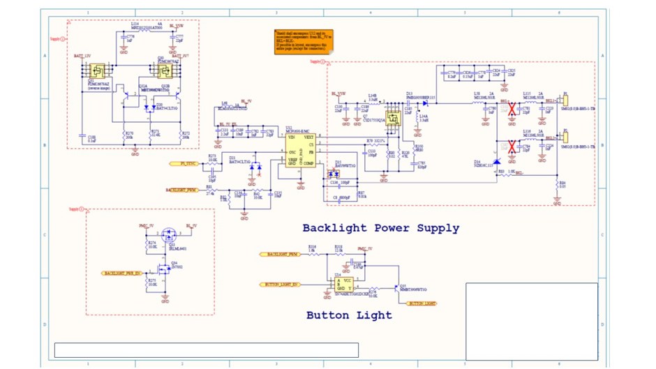
- PCB schematic(s) – Schematics show the electrical design and connectivity of the board, helping engineering teams verify component relationships and troubleshoot issues.
- PCB fabrication drawing and notes – These drawings and notes define the physical board requirements, such as dimensions, materials, stack-up, finishes, tolerances, and special fabrication instructions.
- Assembly drawing(s) – Assembly drawings show how the finished board should be built, including component orientation, polarity, reference locations, and special assembly instructions.
- Test specifications (ICT, Functional, ESS, Hi-Pot, etc.) – Test specifications explain what testing is required, how it should be performed, and what criteria determine pass or fail.
- Quality specifications – Quality specifications outline the workmanship, inspection, and acceptance standards the finished product must meet.
- Regulatory (UL, TUV, etc.) requirements – Regulatory requirements identify any certifications, compliance standards, or documentation needed for the product’s intended market or application.
While a PCA assembly team can quote and build a printed circuit assembly with an abbreviated version of this PCA documentation package, it is not recommended. Detailed documentation for the printed circuit board and printed circuit assembly means a lower probability that an error can pass from the design to the final product. Troubleshooting is also less complicated when the PCA documentation and PCA physical state become comparable “side by side”.
Summary
The successful launch of a new electronic device is often contingent on the PCA documentation. To ensure the highest quality, timely production, and a cost-effective assembly, it is in the best interest of a PCA designer to complete a thorough documentation package for a printed circuit assembly.
Published: April 10, 2018
Last updated: August 22, 2025