Printed circuit boards (PCBs) power nearly all electronic products manufactured today. As such, designers continue to push the limit of PCBs, engineering them to fit integrated circuits and other critical connections that have smaller sizing requirements.
Therefore, to keep up with increasing connectivity demands and rapid electronic manufacturing advancements, PCB assembly manufacturers must conduct thorough quality assurance testing. Manufacturers do tests such as an in-circuit test or x-ray inspection to examine assemblies and detect defects in almost microscopic packages.
Flaws occurring in characteristics definition such as size or power consumption directly impact the individual boards they occur in and risk both the manufacturing process and supply chain. The ultimate manufacturer’s goal is achieving higher production yields at reduced costs and with lower defect rates. Thus, even an occasional defect can undermine this goal.
This article looks at various quality control testing techniques during the electronics manufacturing process.
Six Common PCB Quality Assurance Tests
When you order PCBs, you know the costly consequence of failure. Manufacturers make PCB assembly testing methods an integral part of their manufacturing process. Below is a primer on six essential types of PCB testing.
1 – In Circuit Test (ICT)
An in-circuit test (ICT) is the most robust PCB testing method in existence. The testing technique looks at open circuits, short circuits, component values, and the operation of ICs. It’s a capacitance test.
The bed-of-nail in-circuit test consists of small spring-loaded pogo pins pressed into various testing points to measure resistance. The probes check the integrity of the board’s solder connection. To start the test, you push the board down onto the bed of probes (bed-of-nails). The board has predesigned access points that allow the in-circuit test probes to connect with the circuit.
Manufacturers often perform the ICT on mature products that have few revisions expected. If you lack a design-for-manufacturing testing goal with the proper pads built on your board, you cannot do an ICT. Moreover, you cannot change your mind halfway through production and move into ICT.
2 – Automated Optical Inspection (AOI)
AOI is widely used in manufacturing environments because it is an automatic test that provides a higher degree of speed and repeatability compared to manual inspection methods.
AOI uses either 3D or 2D cameras to snap photos of the PCB before comparing the pictures to a detailed schematic. If a board fails to match the schematic to a particular degree, a technician flags it for inspection.
Never rely on AOI solely. It cannot power up PCBs, and it doesn’t cover all the board’s part types 100 percent. It would be best if you either paired it with a functional, a flying probe, or an in-circuit test.
AOI is particularly useful when you put it at the end of your soldered-boards manufacturing line. Here, the test can quickly locate production problems like solder defects. When you put AOI testing immediately after the soldering process, you can arrest and resolve any issues quickly before they affect subsequently manufactured PCBs.
3 – Flying Probe Test
This non-powered test checks for opens, shorts, capacitance, resistance, inductance, and diode issues. The test utilizes needles attached to an x-y grid probe obtained from basic CAD. Your program then matches the circuit board and checks for errors.
The difference between a flying probe and an in-circuit test is the high initial cost of the latter because you need to design it to fit with the test fixture. However, ICT is a faster and less-error prone test. ICT can also be more cost-effective for more large volume orders compared to the flying probe.
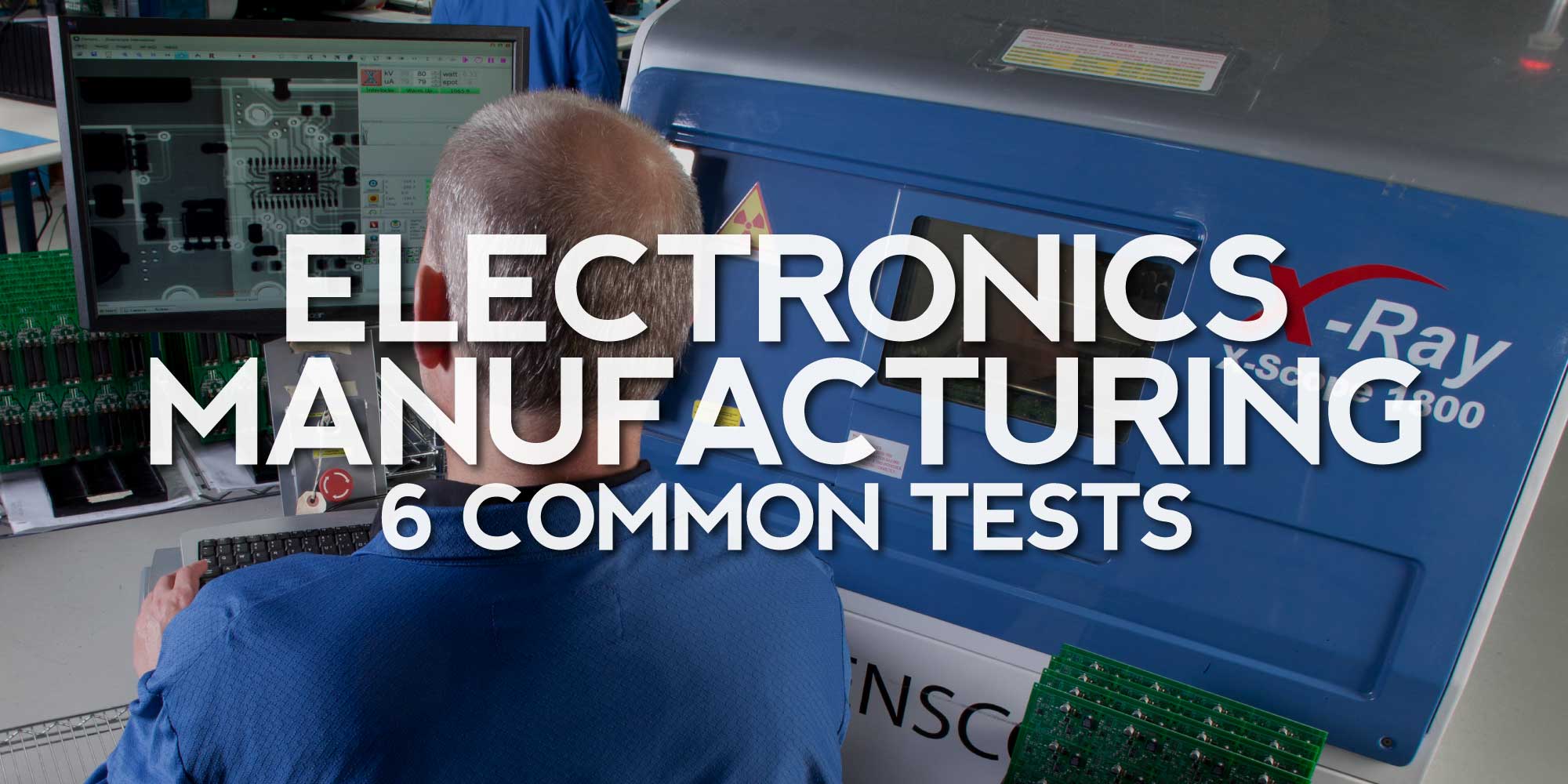
4 – X-Ray Inspection (AXI)
AXI is an inspection tool for most electronics manufacturers. Here, an X-ray technician can locate defects during the manufacturing process by looking at the solder connections, barrels, and internal traces. AXI tests come in 2D and 3D.
X-ray tests can check for elements often hidden from view, for example, ball grid array packages whose solder joint are underneath the chip package. This test requires trained and experienced operators. It is also time-consuming and expensive.
5 – Functional Test
Manufacturers use a functional test to verify that a product powers up. It requires fixtures and external pieces of equipment. It must also meet standard requirements (such as UL and MSHA). Customers usually provide functional tests and their parameters, but manufacturers can help them to design and develop them. Functional testing may take time, but it can save you face and money from a quality and longevity point of view.
6 – Burn-in Test
It’s an intense PCB test that detects early failures and establishes load capacity. Due to its intensity, burn-in testing can destroy other parts. It pushes power continuously through your PCB, usually at the maximum specified capacity, for 48 to 168 hours.
Manufacturers refer to a board failure as infant mortality. This test is necessary for medical or military applications, where boards with high infant mortality are not ideal. This test is not for all projects, and it can shorten a product’s lifespan.
The Bottom Line
PCB testing during the electronics manufacturing process is necessary to detect defective boards and catch issues early before mass production occurs. Don’t overlook PCB prototyping, which also acts as a test that allows you to see the real product before your market does.