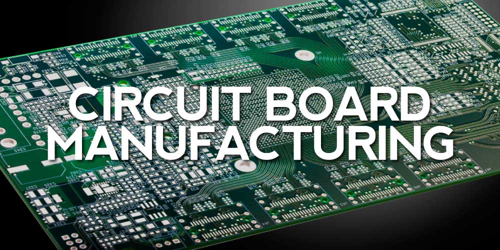
The processes involved to manufacture a Printed Circuit Board (PCB) are time-consuming and complex. Excellence in these processes is imperative because the PCB is the backbone of all electronic circuits. PCB’s come in several different forms; Rigid (hardboard), Flexible (copper and cover-lay), Rigid-flex (hardboard and flex circuits integrated) are the most common. This publication will focus on the processes used to produce Rigid PCB’s which come in 3 varieties: single-sided, double-sided, and multi-layer.
The most commonly used material for rigid PCB’s is based on glass fiber known as FR-4. Other options, like paper phenolic for low-cost commercial products, are used. Teflon or PTFE are used for high performance, high-frequency designs. Flexible, rigid-flex typically use Polyimide based substrates.
The Circuit Board Manufacturing Process
Now, let’s get to the manufacturing process. The printed circuit board manufacturing process can be summarized into the following 13 steps.
1- Design
Before the manufacturing process can begin, the PCB needs to be designed/laid out by a CAD operator based on the working circuit schematic. Once the design process is complete, a set of documents are provided to the PCB manufacturer. Included in the documents are Gerber files, which include a layer by layer configuration, drill files, pick and place data, and text notes. Fabrication Prints, which provide fabrication notes that are critical to the build, all PCB specifications, dimensions, and tolerances.
2- Pre-Manufacturing Prep
Once the PCB house has received the document package from the designer, they are ready to start creating a manufacturing process plan and artwork package. The fabrication specification will determine the plan by calling out things like material type, surface finish, plating, working panel array, process routing, and more. In addition, a physical set of artwork is also created through a film plotter. The artwork will include all layers of the PCB and artwork for solder mask and nomenclature markings.
3- Material Prep
The PCB specification called out by the designer determines the type of material, core thickness, and copper weight used to start material prep. Rigid PCBs that are single-sided and double-sided will not require any inner-layer processing and move directly to the drilling process. If the PCB is a multi-layer, a similar material prep takes place but in the form of inner-layers, which are typically much thinner cores to be built up to a predetermined finished thickness (the stack up).
A common production panel size is 18”x24” but any size can be used if it’s within the PCB manufactures capability.
4- Multi-Layer PCBs Only – Inner Layer Processing
After the inner-layers are prepped in their proper size, material type, core thickness, and copper weight, they are sent to have tooling holes drilled and then printed. The layers are coated on both sides with photoresist. Using the inner-layer artwork and the tooling holes to align both sides, each side is then exposed to UV light detailing the optically negative pattern of traces and features specified for that layer. UV light falling on the photoresist bonds the chemical to the copper surface, and the rest of the unexposed chemical is removed in a developing bath.
The next step is to remove the exposed copper through an etching process. This leaves behind the copper traces hidden under the photoresist layer. During the etching process, the concentration of the etchant and time of exposure are both critical parameters. The resist is then stripped away, leaving traces and features on the inner layers.
Most PCB suppliers use an Automated Optical Inspection system to inspect the layers, and a post-etch punch to optimize the lamination tooling holes.
5- Multi-Layer PCBs Only – Lamination
A predetermined stack up for the process is established during the design process. The lamination process is performed in a cleanroom setting with completed inner-layers, pre-preg, copper foil, press plates, pins, stainless steel dividers, and padding sheets. Depending upon the thickness of the finished PCB, each press stack can hold 4 to 6 boards per press opening. A 4-layer board stack up example is: press plate, steel divider, copper foil (Layer 4), pre-preg, layer 3 – 2 core, pre-preg, copper foil, and repeat. After building the 4 to 6 PCBs, a top press plate is affixed, and into the lamination press goes the bundle. The press is ramp heated, based on a profile, and it applies pressure until the resin melting point at which time the pre-preg flows bonding the multi-layers together, and the press is then cooled. Once removed and prepped, the boards are ready for the drilling process.
6- Drilling
The drilling process is performed by a CNC controlled, multi-station drill machine using high RPM spindles and carbide drill bits specifically designed for PCB drilling. Typical via holes can be as small as .006” to .008” drilled at over 100K RPM.
The drilling process creates a clean, smooth hole-wall that doesn’t damage the inner-layer, but the drilled hole provides an avenue for inner-layer connectivity after plating, and non-via holes eventually are home for thru-hole components.
Non-plated holes are typically drilled as a secondary operation.
7- Copper Plating
Electro-plating is widely used in PCB production where plated through holes are required. The purpose is to deposit a layer of copper through a series of chemical treatment methods onto the conductive substrate, and then increasing the thickness of the copper layer through subsequent electro-plating methods to a specific thickness of design which is usually 1 mil or more.
8- Outer-Layer Processing
Outer-layer processing is virtually the same process and previously described for the inner-layers. The top and bottom layers are coated on both sides with photoresist. Using the outer-layer artwork and the tooling holes to align both sides, each side is then exposed to UV light detailing the optically negative pattern of traces and features. UV light falling on the photoresist bonds the chemical to the copper surface, and the rest of the unexposed chemical is removed in a developing bath. The next step is to remove the exposed copper through an etching process. This leaves behind the copper traces hidden under the photoresist layer. The resist is then stripped away, leaving traces and features on the outer-layers. Automated Optical Inspect can be utilized to find outer-layer defects before the solder mask.
9- Solder-Mask
The application of solder mask is similar to inner and outer layer processes. The main difference is a photo-imageable mask is applied over the entire surface of the production panel instead of a photoresist. The artwork is then used to shoot an image on both the top and bottom layers. Once exposed, the mask is stripped off in the imaged areas. The goal is to expose only the areas where components will be placed and soldered. The mask also limits the surface finish of the PCB to the exposed areas.
10- Surface Finish Plating
There are a few choices for a final surface finish. Gold, Silver, OSP, lead-free solder, leaded solder, to name a few. All are effective, but it really comes down to design requirements. Gold and silver are applied through electro-plating while lead-free solder and leaded solder are applied using a hot air solder level.
11- Nomenclature
Most PCB’s have screened on markings on their surface. The markings are largely for the assembly process, which includes things like reference designators and polarity markings as examples. Other markings can be as simple as part number identification or a manufacturing date code.
12- Depaneling
PCB’s are produced in a full production panel and need to be removed to their manufacturing profile. Most PCB’s are set up in arrays for assembly efficiency. These arrays can be in countless varieties. Too many to describe.
Most arrays are either profile routed on a CNC router using carbide cutters or scored using diamond coated saw-like cutters. Both methods are effective, and the choice of the method is usually determined by the assembly team, which typically approves the array set up in the early stages.
13- Testing
PCB manufacturers generally use flying probe or bed of nails testing process. Methods of testing are determined by product volume and/or equipment available. A test program is created from the net list files, which are included in the original Gerber data. The program will allow the PCB house to test for opens and shorts in the circuits.
About The Author
 Kurt Orr is a Sales Manager at Versa Electronics with a focus on electronic contract manufacturing. Connect with Kurt on LinkedIn.